| CPC H01L 27/0262 (2013.01) [H02H 9/046 (2013.01)] | 20 Claims |
|
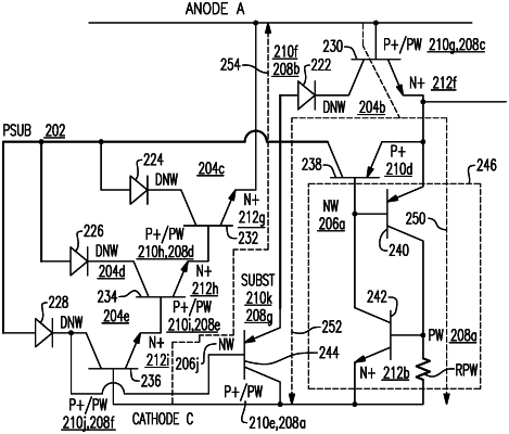
1. An electrical overstress (EOS) protection device comprising:
an anode terminal and a cathode terminal;
a first silicon controlled rectifier (SCR) comprising a first PNP bipolar transistor and a first NPN bipolar transistor that are cross-coupled with a base of the first PNP bipolar transistor connected to a collector of the first NPN bipolar transistor and with a base of the first NPN bipolar transistor is connected to a collector of the first PNP bipolar transistor, wherein an emitter of the first NPN bipolar transistor is connected to the cathode terminal;
a second NPN bipolar transistor including a base connected to the anode terminal and an emitter connected to an emitter of the first PNP bipolar transistor; and
a second PNP bipolar transistor including an emitter connected to an emitter of the second NPN bipolar transistor and a base connected to the base of the first PNP bipolar transistor,
wherein two or more paths for current conduction are present during a positive overstress transient that increases a voltage of the anode terminal relative to the cathode terminal, including a first path through the first SCR and a second path through the second NPN bipolar transistor and the second PNP bipolar transistor.
|