| CPC H01L 27/0255 (2013.01) [H01L 22/20 (2013.01); H01L 27/0292 (2013.01); H01L 21/8249 (2013.01)] | 2 Claims |
|
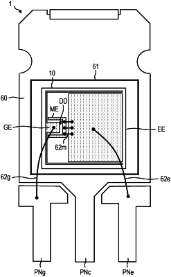
1. A semiconductor device comprising:
a semiconductor chip in which a power device is formed which is an Insulated Gate Bipolar Transistor (IGBT) or a Metal Oxide Semiconductor Field Effect Transistor (MOSFET), the semiconductor chip comprising:
a first electrode coupled to a gate of the power device;
a second electrode coupled to an emitter or a source of the power device;
a third electrode; and
a gate protection element including a first node, a second node and a plurality of stages of p-n junctions formed between the first node and the second node,
wherein, when one of the first electrode and the second electrode is a target electrode and the other is a non-target electrode, the first node is coupled to the third electrode and the second node is coupled to the target electrode, and
wherein the first electrode, the second electrode, the third electrode and the gate protection element are formed in the same semiconductor chip; and
a third wiring member provided outside the semiconductor chip, and coupling the third electrode and the non-target electrode.
|