US 11,942,470 B2
Semiconductor device and method for manufacturing the same
Shih-Wei Peng, Hsinchu (TW); and Jiann-Tyng Tzeng, Hsinchu (TW)
Assigned to TAIWAN SEMICONDUCTOR MANUFACTURING COMPANY, LTD., Hsinchu (TW)
Filed by TAIWAN SEMICONDUCTOR MANUFACTURING COMPANY, LTD., Hsinchu (TW)
Filed on Jan. 17, 2023, as Appl. No. 18/155,536.
Application 18/155,536 is a continuation of application No. 17/135,614, filed on Dec. 28, 2020, granted, now 11,574,901.
Claims priority of provisional application 63/017,357, filed on Apr. 29, 2020.
Prior Publication US 2023/0154916 A1, May 18, 2023
Int. Cl. H01L 27/02 (2006.01); G06F 30/3953 (2020.01); H01L 21/8234 (2006.01); H01L 23/522 (2006.01); H01L 29/06 (2006.01)
CPC H01L 27/0207 (2013.01) [G06F 30/3953 (2020.01); H01L 21/823475 (2013.01); H01L 23/5226 (2013.01); H01L 29/0696 (2013.01)] 20 Claims
OG exemplary drawing
 
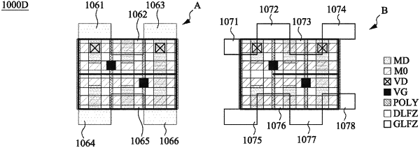
1. A semiconductor device, comprising:
a first cell surrounded by a castle-shaped forbidden region and comprising:
a first active region and a second active region that extend along a first direction and are separated from each other along a second direction traverse to the first direction,
wherein the first active region partially overlaps an upper region of the castle-shaped forbidden region, and the second active region partially overlaps a lower region of the castle-shaped forbidden region; and
at least one via arranged outside the castle-shaped forbidden region.