| CPC H01L 25/50 (2013.01) [H01L 21/568 (2013.01); H01L 23/3121 (2013.01); H01L 24/19 (2013.01); H01L 24/20 (2013.01); H01L 25/0655 (2013.01); H01L 2224/2101 (2013.01)] | 8 Claims |
|
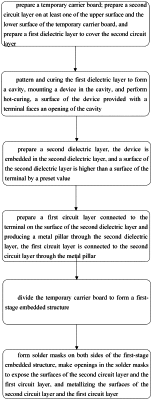
1. A manufacturing method for an embedded structure, comprising:
preparing a temporary carrier board; preparing a second circuit layer on at least one of the upper surface and the lower surface of the temporary carrier board, and preparing a first dielectric layer to cover the second circuit layer;
patterning and curing the first dielectric layer to form a cavity, mounting a device in the cavity, and performing hot-curing, wherein a surface of the device provided with a terminal faces an opening of the cavity;
preparing a second dielectric layer, wherein the device is embedded in the second dielectric layer, and a surface of the second dielectric layer is higher than a surface of the terminal by a preset value;
preparing a first circuit layer connected to the terminal on the surface of the second dielectric layer and producing a metal pillar through the second dielectric layer, wherein the first circuit layer is connected to the second circuit layer through the metal pillar;
dividing the temporary carrier board to form a first-stage embedded structure; and
forming solder masks on both sides of the first-stage embedded structure, making openings in the solder masks to expose the surfaces of the second circuit layer and the first circuit layer, and metallizing the surfaces of the second circuit layer and the first circuit layer.
|