| CPC H01L 25/16 (2013.01) [H01L 21/563 (2013.01); H01L 23/3192 (2013.01); H01L 25/0657 (2013.01); H01L 25/50 (2013.01); H01L 28/40 (2013.01)] | 18 Claims |
|
1. A semiconductor device comprising:
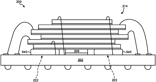
a package substrate having a front side and a backside opposite the front side;
a controller die having a first surface connected to the front side of the package substrate, a second surface opposite the first surface, and a first longitudinal footprint;
a stack of second semiconductor dies on the second surface of the controller die, wherein the stack of second semiconductor dies has a second longitudinal footprint greater than the first longitudinal footprint in at least one dimension;
a passive electrical component on the front side of the package substrate and positioned at least partially within the second longitudinal footprint, wherein the passive electrical component has a first surface contacting the package substrate and a second surface opposite the first surface of the passive electrical component; and
an encapsulant material encasing the passive electrical component, the encapsulant material having an upper surface in a longitudinal plane with the second surface of the controller die and covering the second surface of each passive electrical component such that the encapsulant material contacts a lower surface of the stack of second semiconductor dies,
wherein the encapsulant material and the controller die support the stack of second semiconductor dies.
|