| CPC H01L 25/105 (2013.01) [H01L 21/56 (2013.01); H01L 23/49816 (2013.01); H01L 24/16 (2013.01); H01L 24/20 (2013.01); H01L 24/73 (2013.01); H01L 25/0652 (2013.01); H01L 24/48 (2013.01); H01L 2224/023 (2013.01); H01L 2224/16146 (2013.01); H01L 2224/16235 (2013.01); H01L 2224/2101 (2013.01); H01L 2224/211 (2013.01); H01L 2224/48225 (2013.01); H01L 2224/73209 (2013.01); H01L 2225/06541 (2013.01); H01L 2225/06548 (2013.01); H01L 2225/06572 (2013.01); H01L 2924/181 (2013.01)] | 20 Claims |
|
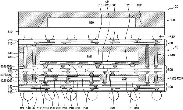
1. A semiconductor package comprising:
a first substrate;
a first semiconductor chip and a passive device which are laterally spaced apart from each other on the first substrate and are disposed face-up on the first substrate;
a first molding part surrounding the first semiconductor chip and the passive device on the first substrate;
a second semiconductor chip disposed on the first molding part and electrically connected to the first semiconductor chip and the passive device;
a second molding part surrounding the second semiconductor chip on the first molding part;
first through-electrodes vertically penetrating the first molding part, at least some of first through-electrodes electrically connecting the first substrate to the second semiconductor chip;
external terminals provided under the first substrate,
wherein the first semiconductor chip comprises:
a base layer;
a circuit layer provided on a top surface of the base layer, the top surface of the base layer facing the second semiconductor chip; and
a via penetrating the base layer to be electrically connected to the circuit layer,
a solder bump connecting the via to the first substrate; and
an adhesive film adhering an inactive surface of the passive device to the first substrate.
|