| CPC H01L 25/0657 (2013.01) [H01L 21/56 (2013.01); H01L 21/76802 (2013.01); H01L 23/31 (2013.01); H01L 23/5384 (2013.01); H01L 23/5386 (2013.01); H01L 24/06 (2013.01); H01L 24/85 (2013.01)] | 17 Claims |
|
1. A semiconductor die assembly, comprising:
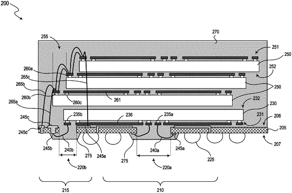
a substrate including a front side and a back side opposite to the front side, wherein the substrate includes a first opening and a second opening;
a first die attached to the front side of the substrate, wherein the first die includes a first side facing toward the front side of the substrate, the first side of the first die including a first bond pad proximate to the first opening and a second bond pad proximate to the second opening;
a first bonding wire coupled to the first bond pad of the first die and extending through the first opening to couple with a first substrate bond pad on the back side of the substrate;
a second bonding wire coupled to the second bond pad of the first die and extending through the second opening to couple with a second substrate bond pad on the back side of the substrate;
one or more second dies disposed over the first die, wherein each of the one or more second dies includes an exposed portion including a third bond pad; and
one or more third bonding wires coupling one or more third bond pads of the one or more second dies with a third substrate bond pad on the front side of the substrate, the third substrate bond pad being directly coupled to the second substrate bond pad by a conductive structure extending through the substrate.
|