| CPC H01L 25/0655 (2013.01) [H01L 23/049 (2013.01); H01L 23/367 (2013.01); H01L 23/5383 (2013.01); H01L 23/642 (2013.01); H01L 24/48 (2013.01); H01L 2224/48225 (2013.01)] | 21 Claims |
|
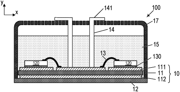
1. A semiconductor module arrangement, comprising:
a housing;
a first semiconductor substrate arranged inside the housing;
a second semiconductor substrate arranged inside the housing;
a first plurality of controllable semiconductor elements; and
a second plurality of controllable semiconductor elements,
wherein:
during operation of the semiconductor module arrangement, each controllable semiconductor element of the first plurality of controllable semiconductor elements generates switching losses and conduction losses, the switching losses being greater than the conduction losses;
during operation of the semiconductor module arrangement, each controllable semiconductor element of the second plurality of controllable semiconductor elements generates switching losses and conduction losses, the conduction losses being greater than the switching losses;
at least a first sub-group of the first plurality of controllable semiconductor elements is arranged on the first semiconductor substrate; and
at least a first sub-group of the second plurality of controllable semiconductor elements is arranged on the second semiconductor substrate.
|