| CPC H01L 24/96 (2013.01) [H01L 21/561 (2013.01); H01L 21/568 (2013.01); H01L 23/544 (2013.01); H01L 23/562 (2013.01); H01L 23/585 (2013.01); H01L 24/24 (2013.01); H01L 24/82 (2013.01); H01L 24/73 (2013.01); H01L 2223/5442 (2013.01); H01L 2223/54426 (2013.01); H01L 2224/24137 (2013.01); H01L 2224/24146 (2013.01); H01L 2224/24265 (2013.01); H01L 2224/73204 (2013.01); H01L 2224/73209 (2013.01); H01L 2224/73217 (2013.01); H01L 2224/82005 (2013.01); H01L 2224/82947 (2013.01)] | 20 Claims |
|
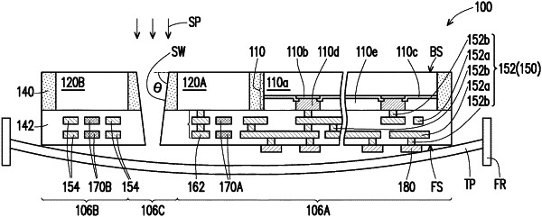
1. A method of forming a semiconductor structure, comprising:
providing a functional die, a first dummy die and a second dummy die, the first dummy die being between the functional die and the second dummy die;
encapsulating the functional die, the first dummy die and the second dummy die by an insulating material;
forming a first alignment mark over the first dummy die and a second alignment mark over the second dummy die, wherein from a top view, a shape of the first alignment mark is different from a shape of the second alignment mark; and
cutting the insulating material along a sawing line between the first alignment mark and the second alignment mark, to separate the functional die and the first dummy die from the second dummy die.
|