| CPC H01L 24/49 (2013.01) [H01L 24/85 (2013.01); H01L 2224/48091 (2013.01); H01L 2224/49096 (2013.01); H01L 2224/4918 (2013.01)] | 11 Claims |
|
1. A semiconductor arrangement, comprising:
a controllable semiconductor element comprising an active region of doped semiconductor material; and
a plurality of bonding wires arranged in parallel to each other in a first horizontal direction,
wherein the active region has a first length in the first horizontal direction and a first width in a second horizontal direction perpendicular to the first horizontal direction,
wherein each of the plurality of bonding wires is electrically and mechanically coupled to a first contact terminal at a top side of the controllable semiconductor element by a first number of bond connections,
wherein each of the bond connections is arranged above the active region in a vertical direction that is perpendicular to the first horizontal direction and the second horizontal direction,
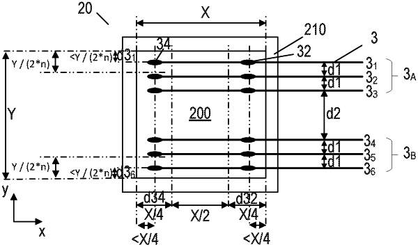
wherein a first bond connection of each of the plurality of bonding wires is arranged at a first distance from a first edge of the active region in the first horizontal direction,
wherein the first distance is less than the first length divided by twice the first number of bond connections,
wherein the first bond connection of each of the plurality of bonding wires is the bond connection arranged closest to the first edge,
wherein a second bond connection of each of the plurality of bonding wires is arranged at a second distance from a second edge of the active region in the first horizontal direction,
wherein the second edge is arranged opposite the first edge,
wherein the second distance is less than the first length divided by twice the first number of bond connections,
wherein the second bond connection of each of the plurality of bonding wires is the bond connection arranged closest to the second edge,
wherein the active region of the controllable semiconductor element is a region configured to carry a current when the controllable semiconductor element is used,
wherein the controllable semiconductor element further comprises an edge region of semiconductor material surrounding the active region in a horizontal plane and that does not carry any currents,
wherein the plurality of bonding wires are electrically and mechanically coupled to the first contact terminal above the active region of the controllable semiconductor element but not the edge region.
|