| CPC H01L 24/48 (2013.01) [H01L 21/4828 (2013.01); H01L 21/565 (2013.01); H01L 23/28 (2013.01); H01L 24/29 (2013.01); H01L 24/32 (2013.01); H01L 2224/04042 (2013.01); H01L 2224/48091 (2013.01); H01L 2224/48177 (2013.01)] | 23 Claims |
|
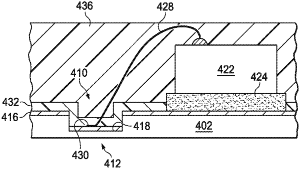
1. A method of fabricating integrated circuits, the method comprising:
providing an electrically conductive die pad having a generally planar top surface;
etching a cavity in the electrically conductive die pad;
attaching a die on the electrically conductive die pad;
attaching a wire bond from the die to a bottom surface of the cavity; and
forming a mold compound over the die and in the cavity.
|