| CPC H01L 24/32 (2013.01) [H01L 23/481 (2013.01); H01L 24/29 (2013.01); H01L 24/83 (2013.01); H01L 25/0657 (2013.01); H01L 25/50 (2013.01); H01L 2224/29188 (2013.01); H01L 2224/32145 (2013.01); H01L 2224/83013 (2013.01); H01L 2224/83896 (2013.01); H01L 2225/06541 (2013.01); H01L 2924/05042 (2013.01); H01L 2924/05442 (2013.01); H01L 2924/3512 (2013.01)] | 20 Claims |
|
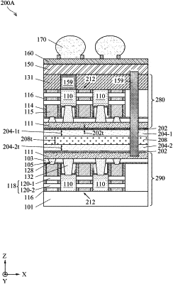
1. A semiconductor structure, comprising:
a first device structure comprising at least one first device and a first storage layer, wherein the first storage layer comprises a porous material containing carbon;
a second device structure comprising at least one second device and a second storage layer, wherein the second storage layer comprises the porous material; and
a bonding layer interposed between the first and second device structures and in contact with the first and second storage layers.
|