| CPC H01L 24/14 (2013.01) [H01L 23/3157 (2013.01); H01L 23/5384 (2013.01); H01L 23/5386 (2013.01); H01L 25/0657 (2013.01); H01L 2224/14181 (2013.01)] | 19 Claims |
|
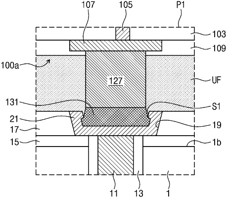
1. A semiconductor package comprising:
at least one second semiconductor chip stacked on a first semiconductor chip; and
an underfill layer interposed between the first semiconductor chip and the at least one second semiconductor chip, the underfill layer is composed of an insulating resin and fillers;
wherein the first semiconductor chip comprises: a first substrate; a first passivation layer disposed on the first substrate, the first passivation layer including a first recess region extending from an uppermost surface of the first passivation layer to a lowermost surface of the first passivation layer; and a first pad covering a bottom surface and sidewalls of the first recess region,
wherein the at least one second semiconductor chip comprises: a second substrate; a second passivation layer disposed adjacent to the first substrate; a conductive bump protruding outside the second passivation layer towards the first semiconductor chip; and an inter-metal compound pattern disposed in the first recess region and positioned between sidewalls of the first pad, a lowermost surface of the inter-metal compound pattern is in direct contact with the first pad in the first recess region and an uppermost surface of the inter-metal compound pattern is in direct contact with the conductive bump,
wherein the underfill layer is in direct contact with both the conductive bump and the inter-metal compound pattern and extends within the first recess region, a lowermost surface of the underfill layer tending within the first recess region is positioned below the uppermost surface of the first passivation layer,
wherein the lowermost surface of the inter-metal compound pattern has a maximum width that is greater than a maximum width of the uppermost surface of the inter-metal compound pattern.
|