| CPC H01L 24/11 (2013.01) [H01L 24/13 (2013.01); H01L 24/81 (2013.01); H01L 2224/1145 (2013.01); H01L 2224/1147 (2013.01); H01L 2224/13026 (2013.01); H01L 2224/13111 (2013.01); H01L 2224/13139 (2013.01); H01L 2224/13144 (2013.01); H01L 2224/13147 (2013.01); H01L 2224/81801 (2013.01)] | 20 Claims |
|
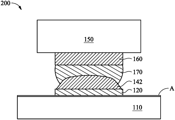
1. A semiconductor device, comprising:
a substrate having a surface;
a conductive pad over a portion of the surface, wherein the conductive pad has a curved top surface, a width of the conductive pad increases toward the substrate, the substrate has a first portion and a second portion adjacent to the first portion, the first portion and the second portion have different thicknesses, and the conductive pad is over the first portion;
a device over the conductive pad; and
a solder layer between the device and the conductive pad, wherein the solder layer covers the curved top surface of the conductive pad, and the conductive pad extends into the solder layer.
|