| CPC H01L 24/08 (2013.01) [H01L 24/05 (2013.01); H01L 24/80 (2013.01); H01L 25/0657 (2013.01); H01L 25/50 (2013.01); H01L 2224/05557 (2013.01); H01L 2224/08146 (2013.01); H01L 2224/80143 (2013.01)] | 20 Claims |
|
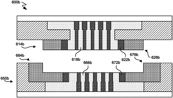
1. A semiconductor device, comprising:
a semiconductor substrate;
a dielectric layer formed over the semiconductor substrate, the dielectric layer having an upper surface; and
an interconnect structure disposed in the dielectric layer, the interconnect structure including:
at least one conductive element electrically coupled to circuitry in the semiconductor substrate, the at least one conductive element having an end surface,
a continuous region of a first insulating material at least partially between the at least one conductive element, the region having an uppermost surface coplanar with the end surface, and
a perimeter structure of a second insulating material surrounding the at least one conductive element and the region of the first insulating material, an uppermost surface of the perimeter structure being vertically offset from the end surface of the at least one conductive element or the upper surface of the dielectric layer.
|