| CPC H01L 23/66 (2013.01) [H01L 21/56 (2013.01); H01L 21/76885 (2013.01); H01L 23/3114 (2013.01); H01L 23/5226 (2013.01); H01L 24/09 (2013.01); H01L 24/17 (2013.01); H01L 24/32 (2013.01); H01L 24/73 (2013.01); H01L 2223/6627 (2013.01); H01L 2223/6677 (2013.01); H01L 2224/0231 (2013.01); H01L 2224/02373 (2013.01); H01L 2224/0401 (2013.01)] | 20 Claims |
|
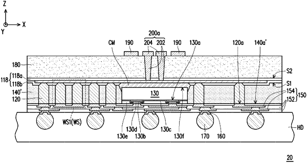
1. A package structure, comprising:
a first redistribution circuit structure and a second redistribution circuit structure;
a semiconductor die, sandwiched between and electrically coupled to the first redistribution circuit structure and the second redistribution circuit structure;
a conductive adhesive, provided between the first redistribution circuit structure and the semiconductor die and extending toward a sidewall of the semiconductor die;
at least one waveguide structure, located aside and electrically coupled to the semiconductor die, wherein the at least one waveguide structure comprises:
a part of the first redistribution circuit structure;
a part of the second redistribution circuit structure; and
a plurality of first through vias, each connecting to the part of the first redistribution circuit structure and the part of the second redistribution circuit structure, wherein a channel is located in the at least one waveguide structure and enclosed by the part of the first redistribution circuit structure, the part of the second redistribution circuit structure and the plurality of first through vias; and
a first antenna, located on the semiconductor die in a stacking direction of the first redistribution circuit structure and the semiconductor die, wherein the first antenna is electrically communicated with the semiconductor die through the at least one waveguide structure.
|