| CPC H01L 23/585 (2013.01) [H01L 21/765 (2013.01); H01L 21/76885 (2013.01); H01L 21/76898 (2013.01); H01L 23/481 (2013.01); H01L 27/0255 (2013.01); H01Q 9/0407 (2013.01)] | 20 Claims |
|
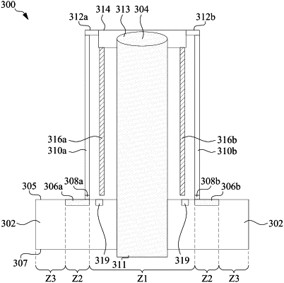
1. A semiconductor device, comprising;
a through-silicon via (TSV) in a TSV zone in a substrate, wherein the TSV extends through the substrate;
an ESD cell proximal to a first end of the TSV and in contact with the TSV zone, the ESD cell comprising a set of diodes electrically connected in parallel to each other;
an antenna pad electrically connected to a second end of the TSV;
an antenna electrically connected to the antenna pad and extending in a first direction, wherein the first direction is parallel to a major axis of the TSV; and
a conductive pillar extending parallel to the TSV at a same side of the substrate as the antenna pad in the first direction, wherein a first end of the conductive pillar electrically connects to the antenna pad, and a second end of the conductive pillar electrically connects to the set of diodes of the ESD cell.
|