| CPC H01L 23/576 (2013.01) [G06F 21/556 (2013.01); G06F 21/78 (2013.01); G06F 21/87 (2013.01); H01L 29/0646 (2013.01); H01L 29/0649 (2013.01); H04L 9/004 (2013.01); H04L 2209/12 (2013.01)] | 18 Claims |
|
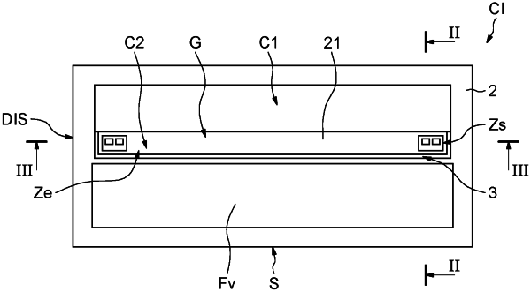
1. An integrated circuit, comprising:
a semiconductor substrate having a rear face and a front face opposite to said rear face;
a first semiconductor well in the semiconductor substrate;
a second semiconductor well in the semiconductor substrate, the second semiconductor well insulated from the first semiconductor well and from a rest of the semiconductor substrate;
wherein the second semiconductor well includes a PN junction; and
a detecting device configured to operate to detect a Differential Fault Analysis (DFA) attack initiated by application of a laser radiation to the semiconductor substrate through detection of a photocurrent flowing in the second semiconductor well, wherein said photocurrent is generate by said PN junction in response to the laser radiation;
wherein the detecting device comprises:
a first isolation trench extending into the second semiconductor well between two locations on a periphery of the second semiconductor well, said first isolation trench having a depth from the front face that is separated by a distance from a bottom of the second semiconductor well;
two contact areas respectively situated on opposite sides of the first trench; and
a detection circuit operating to detect the presence of said photocurrent flowing at one or more of the two contact areas.
|