US 11,942,439 B2
Semiconductor package structure
Tzu-Hung Lin, Hsin-Chu (TW); and Yung-Chang Lien, Hsinchu (TW)
Assigned to MediaTek Inc., Hsin-Chu (TW)
Filed by MediaTek Inc., Hsin-Chu (TW)
Filed on May 13, 2022, as Appl. No. 17/744,297.
Application 17/744,297 is a division of application No. 15/930,645, filed on May 13, 2020, granted, now 11,362,044.
Application 15/930,645 is a continuation in part of application No. 16/813,898, filed on Mar. 10, 2020, granted, now 11,387,176.
Application 15/930,645 is a continuation in part of application No. 15/906,098, filed on Feb. 27, 2018, granted, now 10,784,211.
Claims priority of provisional application 62/818,174, filed on Mar. 14, 2019.
Claims priority of provisional application 62/862,200, filed on Jun. 17, 2019.
Claims priority of provisional application 62/470,915, filed on Mar. 14, 2017.
Prior Publication US 2022/0278055 A1, Sep. 1, 2022
Int. Cl. H01L 23/00 (2006.01); H01L 23/16 (2006.01); H01L 23/31 (2006.01); H01L 23/367 (2006.01); H01L 23/538 (2006.01); H01L 25/065 (2023.01)
CPC H01L 23/562 (2013.01) [H01L 23/16 (2013.01); H01L 23/3185 (2013.01); H01L 23/3675 (2013.01); H01L 23/5383 (2013.01); H01L 23/5385 (2013.01); H01L 23/5386 (2013.01); H01L 24/16 (2013.01); H01L 25/0655 (2013.01); H01L 2224/16235 (2013.01); H01L 2924/19105 (2013.01); H01L 2924/19106 (2013.01); H01L 2924/3511 (2013.01); H01L 2924/3512 (2013.01)] 11 Claims
OG exemplary drawing
 
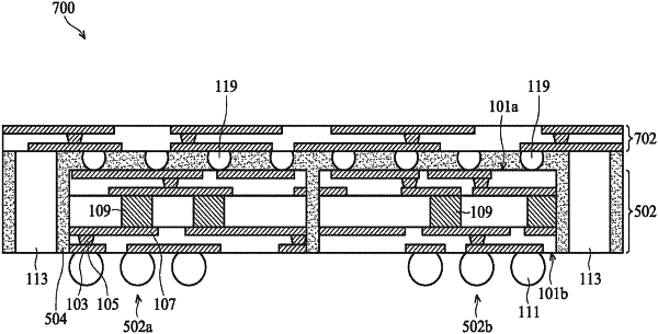
1. A semiconductor package structure, comprising:
a plurality of substrates arranged side-by-side and having a plurality of wiring structures, wherein the plurality of substrates are surrounded by a molding material;
a frame disposed in the molding material and surrounding the plurality of substrates, the plurality of substrates being between portions of the frame;
a redistribution layer disposed over the plurality of substrates and electrically coupled to the plurality of wiring structures; and
a semiconductor die disposed over the redistribution layer.