| CPC H01L 23/552 (2013.01) [H01L 21/56 (2013.01); H01L 21/78 (2013.01); H01L 23/3128 (2013.01); H01L 23/49838 (2013.01); H01L 24/16 (2013.01); H01L 2224/16227 (2013.01)] | 16 Claims |
|
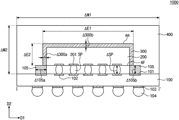
1. A method of fabricating a semiconductor package, the method comprising:
forming an electromagnetic shield that at least partially covers and contacts an upper surface and side surfaces of the semiconductor chip;
forming a molding that at least partially covers the electromagnetic shield; and
electrically connecting the electromagnetic shield to a conductor;
wherein the molding is spaced apart from the semiconductor chip with the electromagnetic shield interposed therebetween.
|