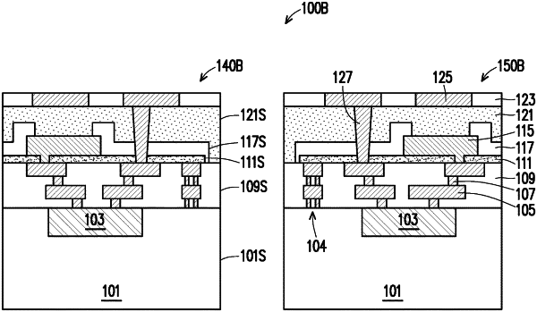
| CPC H01L 23/544 (2013.01) [H01L 21/74 (2013.01); H01L 21/78 (2013.01); H01L 23/3171 (2013.01); H01L 23/525 (2013.01); H01L 23/562 (2013.01); H01L 23/585 (2013.01)] | 20 Claims |

|
1. A semiconductor device comprising:
a substrate;
electrical components in the substrate;
an interconnect structure over the substrate and electrically coupled to the electrical components;
a seal ring around the interconnect structure;
a first passivation layer over the interconnect structure and the seal ring;
a dielectric layer over the first passivation layer, wherein there is a first lateral distance between a first sidewall of the first passivation layer closest to the seal ring and a sidewall of the dielectric layer closest to the seal ring; and
a second passivation layer between the first passivation layer and the interconnect structure, wherein there is a second lateral distance between a second sidewall of the second passivation layer closest to the seal ring and the sidewall of the dielectric layer closest to the seal ring, wherein the first passivation layer extends along an upper surface of the second passivation layer distal from the substrate, and along the second sidewall of the second passivation layer.
|