| CPC H01L 23/5389 (2013.01) [H01L 21/2885 (2013.01); H01L 21/4857 (2013.01); H01L 21/486 (2013.01); H01L 21/56 (2013.01); H01L 21/568 (2013.01); H01L 21/6835 (2013.01); H01L 21/76802 (2013.01); H01L 21/76834 (2013.01); H01L 21/76873 (2013.01); H01L 21/76879 (2013.01); H01L 23/3128 (2013.01); H01L 23/5384 (2013.01); H01L 23/5386 (2013.01); H01L 24/19 (2013.01); H01L 24/24 (2013.01); H01L 25/105 (2013.01); H01L 25/16 (2013.01); H01L 25/50 (2013.01); H01L 23/50 (2013.01); H01L 25/0657 (2013.01); H01L 2221/68331 (2013.01); H01L 2221/68345 (2013.01); H01L 2221/68359 (2013.01); H01L 2221/68372 (2013.01); H01L 2224/04105 (2013.01); H01L 2224/12105 (2013.01); H01L 2224/211 (2013.01); H01L 2224/24265 (2013.01); H01L 2224/32145 (2013.01); H01L 2224/32225 (2013.01); H01L 2224/48091 (2013.01); H01L 2224/48227 (2013.01); H01L 2224/73265 (2013.01); H01L 2224/73267 (2013.01); H01L 2224/92244 (2013.01); H01L 2224/97 (2013.01); H01L 2225/0651 (2013.01); H01L 2225/06568 (2013.01); H01L 2225/06586 (2013.01); H01L 2225/1035 (2013.01); H01L 2225/1041 (2013.01); H01L 2225/1058 (2013.01); H01L 2924/15311 (2013.01); H01L 2924/181 (2013.01); H01L 2924/19011 (2013.01); H01L 2924/19102 (2013.01)] | 20 Claims |
|
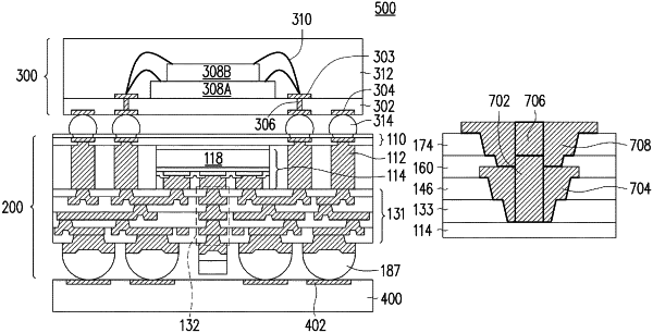
1. A device comprising:
an integrated circuit die comprising a die connector;
a molding compound encapsulating the integrated circuit die;
a first dielectric layer over the molding compound;
a second dielectric layer over the first dielectric layer;
a first conductive pillar extending through the second dielectric layer and the first dielectric layer, the first conductive pillar contacting the die connector; and
a first conductive via around the first conductive pillar, the first conductive via extending through the second dielectric layer and the first dielectric layer.
|