| CPC H01L 23/5389 (2013.01) [H01L 21/4853 (2013.01); H01L 21/4857 (2013.01); H01L 21/565 (2013.01); H01L 21/568 (2013.01); H01L 21/6835 (2013.01); H01L 23/3128 (2013.01); H01L 23/5383 (2013.01); H01L 23/5386 (2013.01); H01L 23/562 (2013.01); H01L 24/19 (2013.01); H01L 24/20 (2013.01); H01L 25/105 (2013.01); H01L 25/50 (2013.01); H01L 2221/68372 (2013.01); H01L 2224/214 (2013.01); H01L 2225/1035 (2013.01); H01L 2225/1052 (2013.01); H01L 2225/1058 (2013.01); H01L 2924/3511 (2013.01)] | 18 Claims |
|
1. A method for manufacturing a semiconductor package, comprising:
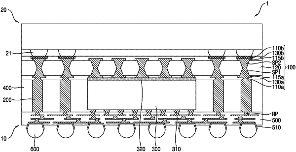
preparing a back-side wiring substrate, wherein the back-side wiring substrate is a printed circuit board (PCB) comprising a core layer, a back-side via plug, a back-side wiring layer, and a back-side pad;
disposing connectors on the back-side pad and on a first surface of the back-side wiring substrate;
disposing a lower semiconductor chip between the connectors on the first surface of the back-side wiring substrate, wherein the lower semiconductor chip comprises a chip bump at an upper surface thereof;
providing an encapsulator on the first surface of the back-side wiring substrate, wherein the encapsulator is on side surfaces of the connectors and the lower semiconductor chip; and
forming a front-side redistribution layer on the encapsulator, on portions of the connectors that are exposed by the encapsulator, and on the chip bump,
wherein a coefficient of thermal expansion of the front-side redistribution layer is greater than a coefficient of thermal expansion of the back-side wiring substrate, and
wherein a modulus of elasticity of the back-side wiring substrate is greater than a modulus of elasticity of the front-side redistribution layer.
|