| CPC H01L 23/5389 (2013.01) [H01L 21/4853 (2013.01); H01L 21/4857 (2013.01); H01L 21/565 (2013.01); H01L 21/568 (2013.01); H01L 21/6835 (2013.01); H01L 23/295 (2013.01); H01L 23/3128 (2013.01); H01L 23/5383 (2013.01); H01L 23/5386 (2013.01); H01L 24/19 (2013.01); H01L 24/20 (2013.01); H01L 25/105 (2013.01); H01L 25/50 (2013.01); H01L 2221/68372 (2013.01); H01L 2224/214 (2013.01); H01L 2225/1035 (2013.01); H01L 2225/1058 (2013.01); H01L 2924/1434 (2013.01); H01L 2924/19106 (2013.01)] | 20 Claims |
|
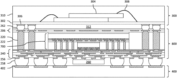
1. A structure comprising:
a first integrated circuit die comprising first die connectors;
a first dielectric layer on the first die connectors;
first conductive vias extending through the first dielectric layer, the first conductive vias connected to a first subset of the first die connectors;
a second integrated circuit die bonded to a second subset of the first die connectors with first reflowable connectors;
a first encapsulant surrounding the second integrated circuit die and the first conductive vias, the first encapsulant comprising a first molding material that extends continuously between the second integrated circuit die and the first conductive vias, the first encapsulant and the first integrated circuit die being laterally coterminous;
second conductive vias adjacent the first integrated circuit die;
a second encapsulant surrounding the second conductive vias, the first encapsulant, and the first integrated circuit die; and
a first redistribution structure comprising first redistribution lines, the first redistribution lines connected to the first conductive vias and the second conductive vias.
|