| CPC H01L 23/5386 (2013.01) [H01L 23/4821 (2013.01); H01L 23/5223 (2013.01); H01L 25/0657 (2013.01); H01L 25/50 (2013.01); H01L 27/0733 (2013.01); H01L 27/0805 (2013.01); H01L 28/40 (2013.01); H01L 28/60 (2013.01); H01L 2224/0603 (2013.01); H01L 2224/8034 (2013.01); H01L 2924/1205 (2013.01); H01L 2924/19041 (2013.01)] | 13 Claims |
|
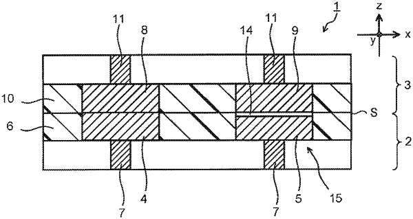
1. A semiconductor device comprising:
a first semiconductor chip including a first metal pad and a second metal pad; and
a second semiconductor chip including a third metal pad and a fourth metal pad, the third metal pad joined to the first metal pad, the fourth metal pad coupled to the second metal pad via an air gap, wherein the second semiconductor chip is coupled to the first semiconductor chip via the first metal pad and the third metal pad,
wherein the first semiconductor chip includes a first semiconductor element and a first wiring layer, a first end of the first wiring layer is coupled to at least one of the first metal pad or the second metal pad, at least a portion of a second end of the first wiring layer is coupled to the first semiconductor element,
the second semiconductor chip includes a second semiconductor element and a second wiring layer, a first end of the second wiring layer is coupled to at least one of the third metal pad or the fourth metal pad, and at least a portion of a second end of the second wiring layer is coupled to the second semiconductor element.
|