| CPC H01L 23/5386 (2013.01) [H01L 21/4846 (2013.01); H01L 21/566 (2013.01); H01L 21/76871 (2013.01); H01L 21/76879 (2013.01); H01L 23/3157 (2013.01); H01L 23/49816 (2013.01); H01L 23/49838 (2013.01); H01L 23/49866 (2013.01); H01L 24/32 (2013.01); H01L 24/48 (2013.01); H01L 25/105 (2013.01); H01L 2224/32145 (2013.01); H01L 2224/48228 (2013.01); H01L 2225/1023 (2013.01); H01L 2225/1052 (2013.01); H01L 2924/1436 (2013.01); H01L 2924/1811 (2013.01); H01L 2924/1815 (2013.01); H01L 2924/182 (2013.01); H01L 2924/183 (2013.01)] | 20 Claims |
|
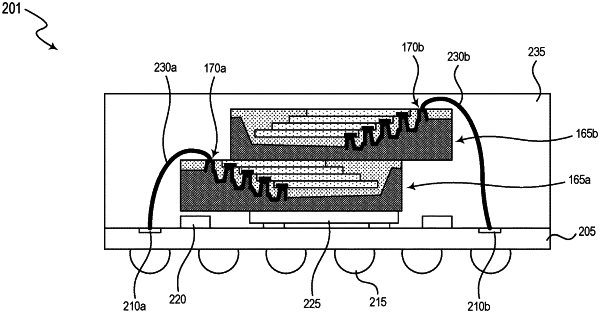
1. A semiconductor die assembly, comprising:
a shingled stack of semiconductor dies, each semiconductor die of the stack including an uncovered porch having one or more bond pads;
a dielectric structure partially encapsulating the shingled stack of semiconductor dies, wherein the dielectric structure includes openings corresponding to the bond pads of the semiconductor dies; and
one or more conductive structures on the dielectric structure, wherein each of the conductive structures extends over at least one porch of the semiconductor dies to connect to the one or more bond pads of the semiconductor dies through corresponding openings of the dielectric structure.
|