| CPC H01L 23/535 (2013.01) [H01L 21/76805 (2013.01); H01L 21/76895 (2013.01); H01L 23/5226 (2013.01); H01L 23/5329 (2013.01); H10B 41/27 (2023.02); H10B 43/27 (2023.02)] | 14 Claims |
|
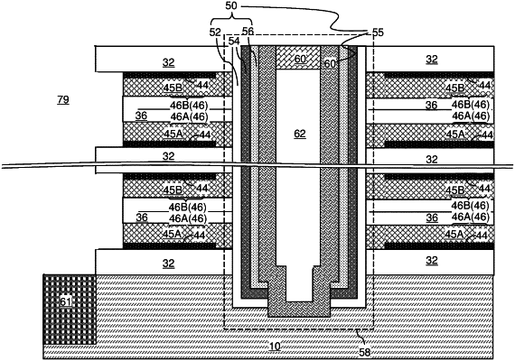
1. A three-dimensional memory device comprising:
a vertical repetition of multiple instances of a unit layer stack, wherein the unit layer stack comprises, from bottom to top, a first-type insulating layer, a first-type electrically conductive layer comprising a first conductive barrier liner and a first conductive fill material layer, a second-type insulating layer, and a second-type electrically conductive layer comprising a second conductive fill material layer and a second conductive barrier liner;
memory openings vertically extending through the vertical repetition; and
memory opening fill structures located within the memory openings, wherein each of the memory opening fill structures comprises a respective vertical stack of memory elements;
wherein:
the first conductive fill material layer and the second conductive fill material layer are in direct contact with horizontal surfaces of the second-type insulating layer;
the first conductive barrier liner is in direct contact with a horizontal surface of the first-type insulating layer; and
the second conductive barrier liner is in direct contact with a horizontal surface of another first-type insulating layer of an adjacent unit layer stack.
|