| CPC H01L 23/5283 (2013.01) [H01L 21/28568 (2013.01); H01L 21/7685 (2013.01); H01L 21/76877 (2013.01); H01L 23/5226 (2013.01); H01L 23/53209 (2013.01); H01L 23/53238 (2013.01); H01L 23/53257 (2013.01)] | 8 Claims |
|
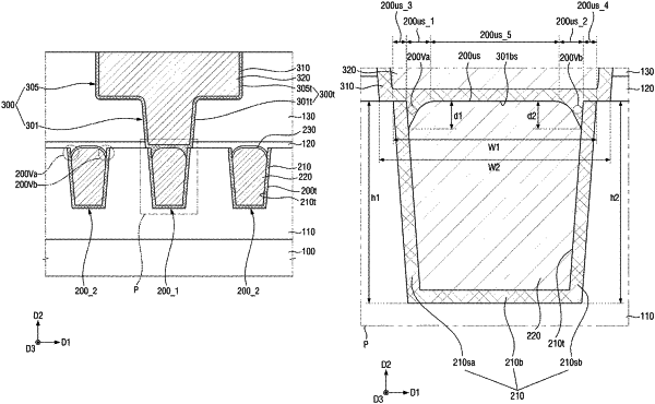
1. A semiconductor device comprising:
a first interlayer insulating film disposed on a substrate and including a first trench;
a first lower conductive pattern filling the first trench and including first and second valley areas that are spaced apart from each other in a first direction parallel to an upper surface of the substrate, the first and second valley areas are recessed toward the substrate and are disposed in the first trench;
a second interlayer insulating film disposed on the first interlayer insulating film and including a second trench that exposes at least a portion of the first lower conductive pattern;
an upper conductive pattern filling the second trench and including an upper barrier film and an upper filling film disposed on the upper barrier fill; and
an etching stopper film disposed between the first and second interlayer insulating films,
wherein the second trench extends into the etching stopper film, and
wherein the upper conductive pattern at least partially fills the first valley area.
|