| CPC H01L 23/5283 (2013.01) [H01L 21/0228 (2013.01); H01L 21/28562 (2013.01); H01L 21/76801 (2013.01); H01L 21/76832 (2013.01); H01L 21/76879 (2013.01); H01L 21/76897 (2013.01); H01L 21/76804 (2013.01)] | 19 Claims |

|
1. A semiconductor structure comprising:
a first dielectric layer comprising a first conductive metal feature embedded in the first dielectric layer;
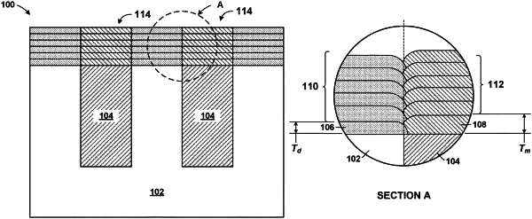
a second dielectric layer comprising a second conductive metal feature embedded in the second dielectric layer, wherein the second dielectric layer comprises a uniform composition throughout, wherein the second conductive metal feature is above and directly contacts the first conductive metal feature, wherein a sidewall of the second dielectric layer comprises a first repeating series of convex curves, and wherein a sidewall of the second conductive metal feature comprises a second repeating series of convex curves; and
an interface between the second conductive metal feature and the second dielectric layer is where the first repeating series of convex curves contact the second repeating series of convex curves.
|
|
7. A semiconductor structure comprising:
a metal nanostructure embedded in a dielectric layer having a uniform composition throughout, wherein a sidewall of the metal nanostructure comprises a series of concave curves, wherein a sidewall of the dielectric layer comprises a series of convex curves; and wherein a boundary between the metal nanostructure and the dielectric layer is where the series of concave curves contact the series of convex curves.
|
|
13. A semiconductor structure comprising:
a conductive nanostructure embedded in a dielectric layer having a uniform composition throughout, wherein a sidewall of the conductive nanostructure comprises a first series of convex and concave curves, wherein a sidewall of the dielectric layer comprises a second series of convex and concave curves; and wherein an interface between the conductive nanostructure and the dielectric layer is where the first series of convex and concave curves contact the second series of convex and concave curves.
|