| CPC H01L 23/528 (2013.01) [G11C 5/063 (2013.01); H01L 23/5283 (2013.01); H10B 12/0335 (2023.02); H10B 12/053 (2023.02); H10B 12/315 (2023.02); H10B 12/34 (2023.02); H10B 12/485 (2023.02)] | 8 Claims |
|
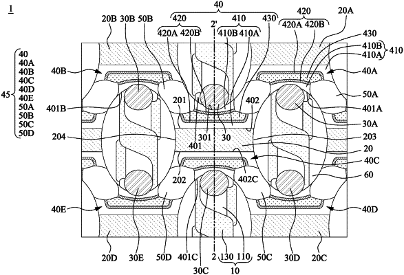
1. A semiconductor structure, comprising:
a semiconductor substrate;
a contact structure on the semiconductor substrate, the contact structure having a first side and a second side opposite to the first side;
a dielectric spacer adjacent to the contact structure and having a first concave surface; and
a first conductive element on the semiconductor substrate, wherein the first conductive element is partially surrounded by the first concave surface of the dielectric spacer;
wherein the dielectric spacer comprises:
a first dielectric layer at the first side of the contact structure;
a second dielectric layer on the first dielectric layer, wherein the second dielectric layer has a U-shape structure from a top view perspective; and
a third dielectric layer on the second dielectric layer, wherein the third dielectric layer has a U-shape structure from a top view perspective.
|