| CPC H01L 23/528 (2013.01) [H01L 21/76224 (2013.01); H01L 21/76802 (2013.01); H01L 21/76819 (2013.01); H01L 23/53214 (2013.01); H01L 23/53257 (2013.01); H01L 23/5329 (2013.01); H01L 21/7682 (2013.01); H01L 23/5222 (2013.01)] | 10 Claims |
|
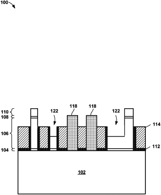
1. An interconnect structure comprising:
one or more metal lines in direct contact with a top surface of one or more devices;
one or more vias in direct contact with top surfaces of the one or more metal lines; and
one or more dielectric pillars in direct contact with the top surface of the one or more devices, wherein a height of a top surface of the one or more dielectric pillars above the one or more device is equal to a height of a top surface of the one or more vias above the one or more devices, and wherein the top surface of the one or more vias and the top surface of the one or more dielectric pillars are configured to act as a chemical-mechanical planarization stop based on a spacing of the one or more metal lines and the one or more dielectric pillars across the interconnect structure.
|