|
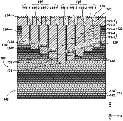
20. A method of forming a microelectronic device, comprising: forming a stack structure comprising insulative structures and additional structures vertically interleaved with the insulative structures, the insulative structures and the additional structures arranged in tiers individually comprising one of the insulative structures and one of the additional structures; forming a trench vertically extending through some of the tiers of the stack structure; forming a horizontally alternating sequence of insulative spacer structures and liner structures with a horizontal area of the trench, a material composition of the liner structures is substantially the same as a material composition of the additional structures, and pairs of the liner structures horizontally adjacent opposing sides of respective ones of the insulative spacer structures in contact with different respective ones of the additional structures of the stack structure than one another; and selectively replacing material of the liner structures and the additional structures of the stack structure with conductive material to substantially simultaneously form conductive contact structures from the liner structures and conductive structures from the additional structures, each of the conductive contact structures integral and continuous with a respective one of the conductive structures.
|