| CPC H01L 23/5226 (2013.01) [H01L 23/528 (2013.01); H10B 43/27 (2023.02); H10B 43/35 (2023.02); H10B 43/40 (2023.02)] | 3 Claims |
|
1. A semiconductor memory device comprising:
a semiconductor substrate;
a memory cell array disposed separately from the semiconductor substrate in a first direction intersecting with a surface of the semiconductor substrate;
first and second wirings disposed in the first direction of the memory cell array, the first and second wirings having a distance from the semiconductor substrate larger than a distance of the memory cell array from the semiconductor substrate; and
a fifth wiring disposed separately from the memory cell array in the first direction, the fifth wiring having a distance from the semiconductor substrate smaller than a distance of the memory cell array from the semiconductor substrate, wherein
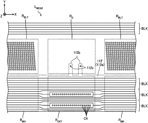
the semiconductor substrate includes a first region to a third region arranged in order in a second direction intersecting with the first direction and a fourth region to a sixth region arranged in order in the second direction, wherein
in a third direction intersecting with the first direction and the second direction:
the fourth region is adjacent to the first region;
the fifth region is adjacent to the second region; and
the sixth region is adjacent to the third region; wherein
the memory cell array includes:
a plurality of first conducting layers extending in the second direction over the first region, the second region, and the third region, the plurality of first conducting layers being laminated in the first direction together with a plurality of first insulating layers in alternation;
a plurality of second insulating layers extending in the second direction over the fourth region, the fifth region, and the sixth region, the plurality of second insulating layers being laminated in the first direction together with the plurality of first insulating layers in alternation;
a first semiconductor layer disposed over the first region, the first semiconductor layer extending in the first direction and being opposed to the plurality of first conducting layers;
a second semiconductor layer disposed over the third region, the second semiconductor layer extending in the first direction and being opposed to the plurality of first conducting layers;
a first contact disposed above the fourth region, the first contact extending in the first direction and being opposed to the plurality of second insulating layers;
a second contact disposed above the sixth region, the second contact extending in the first direction and being opposed to the plurality of second insulating layers; and
a second conducting layer disposed between the plurality of first conducting layers and the semiconductor substrate, the second conducting layer including a first part and a second part, wherein
the first part of the second conducting layer extends in the second direction over the first region, the second region, and the third region, and the first part is connected to the first semiconductor layer above the first region and connected to the second semiconductor layer above the third region,
the second part of the second conducting layer extends over parts of the second region and the fifth region,
the first wiring extends in the third direction over parts of the first region and the fourth region, and the first wiring is electrically connected to the first semiconductor layer and connected to the first contact,
the second wiring extends in the third direction over parts of the third region and the sixth region, and the second wiring is electrically connected to the second semiconductor layer and connected to the second contact, and
the fifth wiring electrically connects the second part of the second conducting layer to the semiconductor substrate.
|