US 11,942,419 B2
Etch stop layer in integrated circuits
Shiu-Ko JangJian, Tainan (TW); Tsung-Hsuan Hong, Tainan (TW); Chun Che Lin, Tainan (TW); and Chih-Nan Wu, Tainan (TW)
Assigned to Taiwan Semiconductor Manufacturing Company, Ltd., Hsin-Chu (TW)
Filed by Taiwan Semiconductor Manufacturing Co., Ltd., Hsinchu (TW)
Filed on Jun. 30, 2022, as Appl. No. 17/809,914.
Application 15/244,961 is a division of application No. 14/689,929, filed on Apr. 17, 2015, granted, now 9,437,484, issued on Sep. 6, 2016.
Application 17/809,914 is a continuation of application No. 16/933,551, filed on Jul. 20, 2020, granted, now 11,404,368.
Application 16/933,551 is a continuation of application No. 16/148,076, filed on Oct. 1, 2018, granted, now 10,720,386, issued on Jul. 21, 2020.
Application 16/148,076 is a continuation of application No. 15/244,961, filed on Aug. 23, 2016, granted, now 10,090,242, issued on Oct. 2, 2018.
Claims priority of provisional application 62/065,459, filed on Oct. 17, 2014.
Prior Publication US 2022/0336348 A1, Oct. 20, 2022
This patent is subject to a terminal disclaimer.
Int. Cl. H01L 23/522 (2006.01); H01L 21/768 (2006.01); H01L 23/532 (2006.01)
CPC H01L 23/5226 (2013.01) [H01L 21/76802 (2013.01); H01L 21/76807 (2013.01); H01L 21/76826 (2013.01); H01L 21/76829 (2013.01); H01L 21/76832 (2013.01); H01L 21/76834 (2013.01); H01L 21/76877 (2013.01); H01L 23/53238 (2013.01); H01L 23/5329 (2013.01); H01L 23/53295 (2013.01); H01L 21/76849 (2013.01); H01L 2924/0002 (2013.01)] 20 Claims
OG exemplary drawing
 
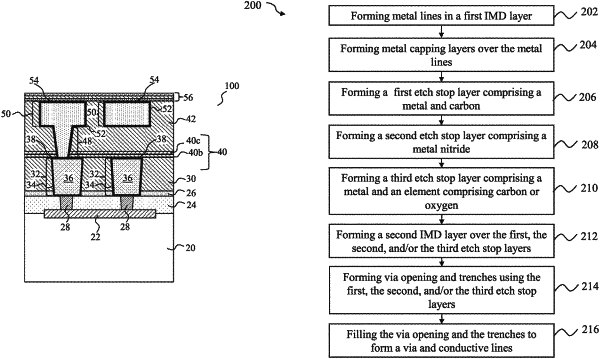
1. A method comprising:
forming a conductive feature;
forming an etch stop layer over the conductive feature, wherein the forming the etch stop layer comprises:
depositing a first aluminum compound dielectric layer;
depositing a middle layer over the first aluminum compound dielectric layer; and
forming a second aluminum compound dielectric layer over the middle layer, wherein the forming the second aluminum compound dielectric layer comprises, after the middle layer is deposited, performing a treatment process on a top sub layer of the middle layer to form the second aluminum compound dielectric layer, wherein a bottom sub layer of the middle layer remains as the middle layer; and
forming a dielectric layer over the etch stop layer.