| CPC H01L 23/5226 (2013.01) [H01L 21/768 (2013.01); H01L 23/528 (2013.01); H01L 24/14 (2013.01)] | 20 Claims |
|
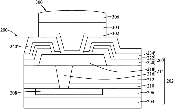
1. A semiconductor structure comprising:
a combined feature including a passivation layer, a contact via extending through the passivation layer, a conductive pad disposed on and connected to the contact via, and a dielectric layer disposed on the passivation layer and the conductive pad;
a bump feature disposed on the combined feature and connected to the conductive pad;
a protection layer disposed on the dielectric layer and surrounding a lower portion of the bump feature; and
a fluorine-containing polymeric layer disposed on the protection layer, surrounding at least a part of the lower portion of the bump feature, and separated from the conductive pad by the protection layer,
wherein the protection layer includes a first sub-layer that is in direct contact with the conductive pad, and a second sub-layer that is in direct contact with the fluorine-containing polymeric layer, one of the first sub-layer and the second sub-layer being made of an oxide material, the other one of the first sub-layer and the second sub-layer being made of a nitride material.
|