| CPC H01L 23/49844 (2013.01) [H01L 24/48 (2013.01); H01L 25/115 (2013.01); H02M 7/003 (2013.01); H01L 2224/48225 (2013.01); H02M 7/5387 (2013.01)] | 12 Claims |
|
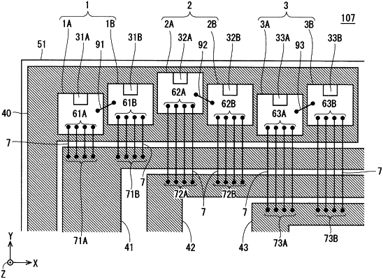
1. A semiconductor device comprising:
a common circuit pattern; and
a plurality of semiconductor chips arranged along a first direction on the common circuit pattern,
wherein each of the plurality of semiconductor chips includes a switching element, a first main electrode of the switching element is provided on an upper surface, a second main electrode of the switching element is provided on a lower surface, and a part of a first main electrode is allocated to a wiring connection region,
the semiconductor device further comprises
a plurality of external wiring lines each of which is electrically connected to the wiring connection region of a corresponding semiconductor chip among the plurality of semiconductor chips,
wherein a pair of semiconductor chips adjacent to each other in the first direction among the plurality of semiconductor chips satisfies both of first and second arrangement conditions,
the first arrangement condition is that the pair of semiconductor chips is separately arranged without the wiring connection regions overlapping each other in a second direction intersecting the first direction, and
the second arrangement condition is that, in the second direction, the pair of semiconductor chips is arranged to partially overlap so that a part of regions other than the wiring connection regions overlap.
|