| CPC H01L 23/49838 (2013.01) [H01L 21/3043 (2013.01); H01L 21/768 (2013.01); H01L 22/34 (2013.01); H01L 23/528 (2013.01); H01L 25/0655 (2013.01)] | 18 Claims |
|
1. An integrated circuit comprising:
a first set of dies, each die comprising circuitry; and
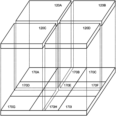
a second set of interposer dies, the second set of interposer dies collectively having a smaller perimeter than a collective perimeter of the first set of dies, at least two dies of the first set of dies being connected to each other via at least one of the interposer dies, the at least one of the interposer dies including first connections connected to a first die of the first set of dies, second connections connected to a second die of the first set of dies, and buffers connected between the first connections and the second connections, the buffers being configured to condition signals between the first die and the second die.
|