| CPC H01L 23/49827 (2013.01) [H01L 21/76877 (2013.01); H01L 21/76898 (2013.01); H01L 23/481 (2013.01)] | 12 Claims |
|
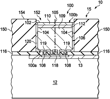
1. A method, comprising:
forming an insulating member over a circuit on a device side of a semiconductor die;
removing a portion of the insulating member to produce a cavity;
forming a seed layer on the insulating member and within the cavity;
forming a conductive member on the seed layer in the cavity, wherein the conductive member comprises a plurality of layers of different metal materials; and
removing the seed layer from atop the insulating member, outside the cavity, after forming the conductive member in the cavity such that a remaining portion of the seed layer is positioned between the conductive member and the insulating member, wherein the seed layer abuts an outer perimeter of the conductive member.
|