| CPC H01L 23/49816 (2013.01) [H01L 23/49827 (2013.01); H01L 25/0657 (2013.01); H01L 25/105 (2013.01); H01L 23/13 (2013.01); H01L 24/16 (2013.01); H01L 24/48 (2013.01); H01L 2224/16235 (2013.01); H01L 2224/48105 (2013.01); H01L 2224/48227 (2013.01); H01L 2224/4824 (2013.01); H01L 2225/06506 (2013.01); H01L 2225/06541 (2013.01); H01L 2225/06562 (2013.01); H01L 2225/1058 (2013.01); H01L 2225/107 (2013.01); H01L 2924/14361 (2013.01)] | 21 Claims |
|
1. An apparatus, comprising:
a device substrate comprising a semiconductor material and bond pads coupled with an active surface of the device substrate;
a package substrate secured to the device substrate, the package substrate configured to route signals to and from the bond pads; and
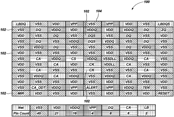
a ball grid array supported on, and electrically connected to, the package substrate, the ball grid array comprising an odd number of columns, such that the ball grid array comprises a central column having equal numbers of other columns on opposite sides of the central column;
wherein each ball of the ball grid array positioned and configured to carry a clock signal or a strobe signal is located in the central column of the ball grid, array,
wherein a total number of balls in the ball grid array is between about 115 and about 120.
|