| CPC H01L 23/49568 (2013.01) [H01L 23/315 (2013.01); H01L 23/49575 (2013.01); H01L 2224/48091 (2013.01); H01L 2224/48247 (2013.01); H01L 2924/183 (2013.01)] | 20 Claims |
|
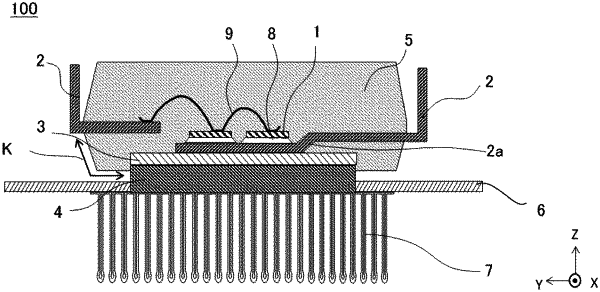
1. A semiconductor apparatus comprising:
a semiconductor device;
a lead frame to which the semiconductor device is bonded;
an insulating layer on which the lead frame is provided;
a metal base plate provided on a face of the insulating layer opposite to a face on which the lead frame is provided;
a sealing member to seal the semiconductor device, the lead frame, the insulating layer, and the metal base plate in such a way that a portion of the lead frame and at least one portion of the metal base plate are exposed;
a support frame having at least one opening in which the at least one exposed portion of the metal base plate exposed from the sealing member is inserted; and
a heat dissipating member that is provided with multiple fins formed by folding a metal plate and that is welded to a part of the at least one exposed portion of the metal base plate inserted in the at least one opening and to the support frame.
|