| CPC H01L 23/427 (2013.01) [H01L 23/481 (2013.01); H01L 23/49816 (2013.01); H01L 23/49822 (2013.01); H01L 23/49833 (2013.01); H01L 23/49838 (2013.01); H01L 24/16 (2013.01); H01L 25/0655 (2013.01); H01L 2224/16235 (2013.01)] | 16 Claims |
|
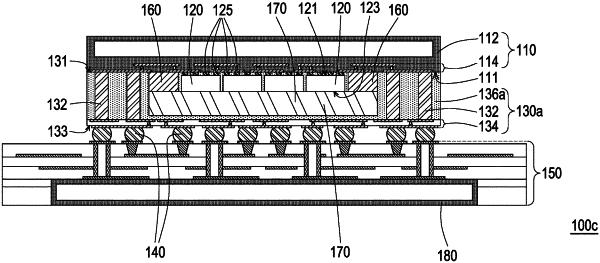
1. A heterogeneous integration semiconductor package structure, comprising:
a heat dissipation assembly, having a connection surface, and comprising a two-phase flow heat dissipation device and a first redistribution structure layer embedded in the connection surface;
a plurality of chips, disposed on the connection surface of the heat dissipation assembly and electrically connected to the first redistribution structure layer;
a package assembly, disposed on the connection surface of the heat dissipation assembly and surrounding the chips, wherein the package assembly has an upper surface adjacent to the connection surface and a lower surface opposite to the upper surface and comprises a second redistribution structure layer disposed on the lower surface and a plurality of conductive vias electrically connected to the first redistribution structure layer and the second redistribution structure layer;
a plurality of connectors, disposed on the package assembly, and electrically connected to the second redistribution structure layer;
a circuit substrate, electrically connected to the second redistribution structure layer of the package assembly through the connectors;
a plurality of solder balls, disposed between the chips and the first redistribution structure layer, wherein the chips are electrically connected to the first redistribution structure layer through the solder balls, wherein the package assembly further comprises a package component wrapping a periphery of the chips and a periphery of the conductive vias, connected to the first redistribution structure layer and the second redistribution structure layer, and filled between the solder balls and the chips;
a plurality of heat conduction blocks, disposed on the connection surface of the heat dissipation assembly, surrounding the periphery of the chips and a periphery of the solder balls, and connected to the first redistribution structure layer; and
a heat conduction device, in contact with the heat conduction blocks and the chips, wherein the chips and the heat conduction blocks are located between the heat conduction device and the heat dissipation assembly, and the package component further wraps a periphery of the heat conduction blocks and a periphery of the heat conduction device.
|