| CPC H01L 23/315 (2013.01) [H01L 21/565 (2013.01); H01L 23/3114 (2013.01); H01L 24/16 (2013.01); H01L 25/10 (2013.01); H01L 25/50 (2013.01); H01L 2224/16145 (2013.01)] | 15 Claims |
|
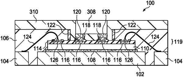
1. A semiconductor package, comprising:
a wafer chip scale package (WCSP) having a circuitry formed in a device side and an insulative layer above the device side;
a wall extending vertically to form a defined space, the wall configured to prevent mold compound from flowing into the defined space;
a mold compound abutting surfaces of the wall opposing the defined space; and
a conductive terminal coupled to the circuitry and extending from the WCSP into the defined space.
|