| CPC H01L 23/315 (2013.01) [H01L 21/4825 (2013.01); H01L 21/565 (2013.01); H01L 23/49513 (2013.01); H01L 23/4952 (2013.01); H01L 23/49575 (2013.01); H01L 24/02 (2013.01); H01L 24/13 (2013.01); H01L 24/16 (2013.01); H01L 24/48 (2013.01); H01L 24/73 (2013.01); H01L 2224/0239 (2013.01); H01L 2224/024 (2013.01); H01L 2224/13082 (2013.01); H01L 2224/13111 (2013.01); H01L 2224/13139 (2013.01); H01L 2224/13147 (2013.01); H01L 2224/16145 (2013.01); H01L 2224/48137 (2013.01); H01L 2224/48245 (2013.01); H01L 2224/48465 (2013.01); H01L 2224/73207 (2013.01); H01L 2924/01028 (2013.01); H01L 2924/01029 (2013.01); H01L 2924/01074 (2013.01); H01L 2924/07025 (2013.01); H01L 2924/19104 (2013.01)] | 17 Claims |
|
1. A semiconductor device, comprising:
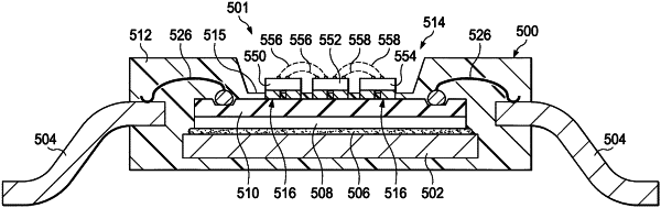
a semiconductor package including a mold compound covering a semiconductor die, the semiconductor package having a surface and a cavity in the surface, the semiconductor die having a device side facing the cavity, the device side having circuitry therein; and
an electronic device positioned within the cavity, the electronic device coupled to the semiconductor die via a conductive terminal extending through the mold compound, the conductive terminal having a first end physically contacting the device side and a second end extending into the cavity, and wherein the conductive terminal comprises a copper post, and wherein the electronic device includes another semiconductor die.
|