| CPC H01L 23/3135 (2013.01) [H01L 21/565 (2013.01); H01L 23/291 (2013.01); H01L 23/295 (2013.01); H01L 23/3121 (2013.01); H01L 23/5387 (2013.01); H01L 24/16 (2013.01); H01L 24/81 (2013.01); H01L 25/0652 (2013.01); H01L 2224/16227 (2013.01); H01L 2225/06517 (2013.01); H01L 2225/06572 (2013.01); H01L 2924/351 (2013.01)] | 14 Claims |
|
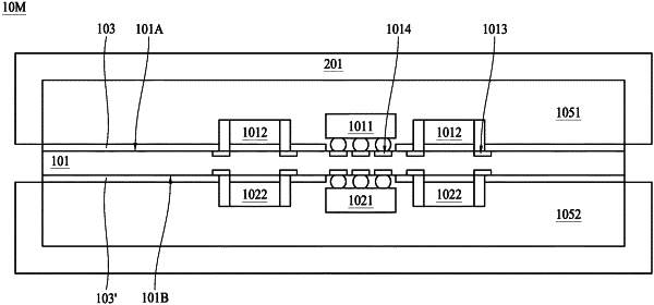
1. A semiconductor package, comprising:
a substrate having a first side and a second side opposite to the first side;
a first semiconductor die disposed on the first side of the substrate;
a second semiconductor die disposed on the second side of the substrate;
a first compound encapsulating the first semiconductor die;
a second compound encapsulating the second semiconductor die; and
a display disposed over a first side of the substrate and electrically connected to the first semiconductor dies, wherein the display is laterally encapsulated by the first compound, and wherein a top surface of the display is at least partially exposed from the first compound.
|