| CPC H01L 23/3107 (2013.01) [H01L 23/4952 (2013.01); H01L 24/16 (2013.01); H01L 24/48 (2013.01); H01L 2224/16245 (2013.01); H01L 2224/48245 (2013.01)] | 22 Claims |
|
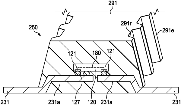
1. A semiconductor package, comprising:
a leadframe including a plurality of leads;
a semiconductor die including bond pads attached to the leadframe with the bond pads electrically coupled to the plurality of leads, the semiconductor die comprising a substrate having a semiconductor surface including circuitry having nodes coupled to the bond pads, and
a mold compound encapsulating the semiconductor die that is interdigitated comprising alternating extended mold regions over the plurality of leads and recessed mold regions in between adjacent ones of the plurality of leads, at least one of the extended mold regions extending from a top surface to a bottom surface of the mold compound.
|