US 11,942,380 B2
Semiconductor structure and testing method thereof
Ming-Shiang Lin, Hsinchu (TW); Chia-Cheng Ho, Hsinchu (TW); Chun-Chieh Lu, Taipei (TW); Cheng-Yi Peng, Taipei (TW); and Chih-Sheng Chang, Hsinchu (TW)
Assigned to TAIWAN SEMICONDUCTOR MANUFACTURING CO., LTD., Hsinchu (TW)
Filed by TAIWAN SEMICONDUCTOR MANUFACTURING CO., LTD., Hsinchu (TW)
Filed on Oct. 26, 2020, as Appl. No. 17/080,625.
Application 17/080,625 is a continuation of application No. 16/020,860, filed on Jun. 27, 2018, granted, now 10,818,562.
Claims priority of provisional application 62/593,124, filed on Nov. 30, 2017.
Prior Publication US 2021/0057290 A1, Feb. 25, 2021
Int. Cl. H01L 29/417 (2006.01); G01R 27/26 (2006.01); H01L 21/283 (2006.01); H01L 21/306 (2006.01); H01L 21/324 (2006.01); H01L 21/66 (2006.01); H01L 29/66 (2006.01)
CPC H01L 22/14 (2013.01) [G01R 27/2617 (2013.01); H01L 22/34 (2013.01)] 20 Claims
OG exemplary drawing
 
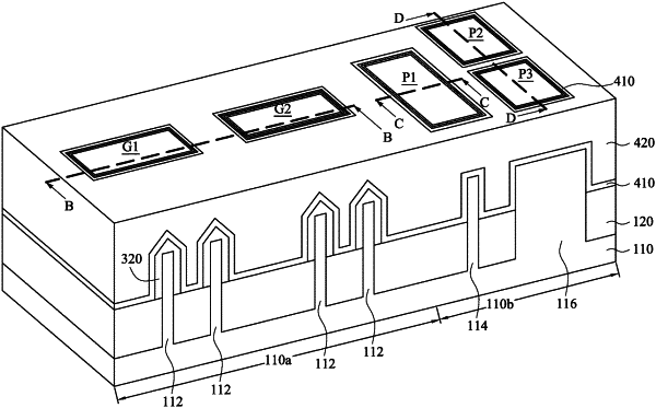
1. A method, comprising:
forming a dummy pattern over a test region of a substrate;
forming an interlayer dielectric (ILD) layer laterally surrounding the dummy pattern;
removing the dummy pattern to form an opening;
forming a dielectric layer in the opening;
performing a first testing process on the dielectric layer;
performing an annealing process to the dielectric layer; and
performing a second testing process on the annealed dielectric layer.