| CPC H01L 21/8252 (2013.01) [H01L 27/0605 (2013.01); H01L 29/045 (2013.01); H01L 29/267 (2013.01); H01L 29/66462 (2013.01); H01L 29/73 (2013.01); H01L 29/778 (2013.01)] | 20 Claims |
|
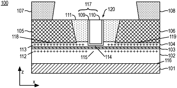
1. A transistor structure, comprising:
a first crystalline material layer comprising group III atoms and nitrogen;
a second crystalline material layer comprising group III atoms and nitrogen;
a layer other than a III-N material between the first and second crystalline material layers, wherein the first crystalline material layer comprises a first crystal orientation and the second crystalline material layer comprises a second crystal orientation inverted with respect to the first crystal orientation; and
a source, a drain, and a gate coupled to the first crystalline material layer.
|