| CPC H01L 21/823842 (2013.01) [H01L 21/32134 (2013.01); H01L 21/823821 (2013.01); H01L 27/0924 (2013.01); H01L 29/401 (2013.01); H01L 29/42372 (2013.01)] | 20 Claims |
|
1. A semiconductor device, comprising:
a semiconductor substrate;
a plurality of channel regions, including a p-type channel region, an n-type channel region, and a third channel region disposed over the semiconductor substrate; and
a gate structure comprising:
a gate dielectric layer disposed over the plurality of channel regions;
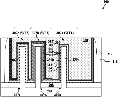
a work function metal (WFM) structure disposed over the gate dielectric layer, wherein the WFM structure includes an n-type WFM layer over the n-type channel region and not over the p-type channel region or the third channel region and further includes a p-type WFM layer over both the n-type WFM layer and the p-type channel region and not the third channel region; and
a fill metal layer.
|