| CPC H01L 21/823821 (2013.01) [H01L 21/265 (2013.01); H01L 21/324 (2013.01); H01L 21/823814 (2013.01); H01L 21/823828 (2013.01); H01L 21/823871 (2013.01); H01L 27/0924 (2013.01); H01L 29/66795 (2013.01); H01L 29/785 (2013.01); H01L 21/26506 (2013.01); H01L 21/268 (2013.01); H01L 21/28518 (2013.01)] | 20 Claims |
|
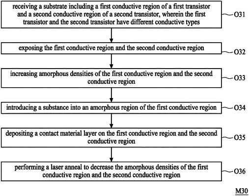
1. A method for manufacturing a semiconductor structure, comprising:
receiving a substrate including a first conductive region and a first gate structure of a first transistor and a second conductive region and a second gate structure of a second transistor, wherein the first transistor and the second transistor have different conductive types;
consuming a thickness of a first spacer on a vertical surface of the first gate structure and a thickness of a second spacer on a vertical surface of the second gate structure;
forming a liner layer over the first spacer and the second spacer;
performing an amorphization on the first conductive region and the second conductive region concurrently by a first implantation;
performing a second implantation to introduce a P-type dopant on the first conductive region;
forming a contact material layer over the first conductive region and the second conductive region, wherein the first conductive region is implanted by the first implantation and the second implantation prior to the formation of the contact material layer, and the second conductive region is implanted by the first implantation prior to the formation of the contact material layer;
performing a thermal anneal on the first conductive region and the second conductive region; and
performing a laser anneal on the first conductive region and the second conductive region.
|