| CPC H01L 21/823821 (2013.01) [H01L 21/02532 (2013.01); H01L 21/823807 (2013.01); H01L 21/823814 (2013.01); H01L 21/823842 (2013.01); H01L 21/823871 (2013.01); H01L 27/0924 (2013.01); H01L 27/0928 (2013.01); H01L 29/66545 (2013.01); H01L 29/66795 (2013.01); H01L 29/785 (2013.01); H01L 21/823892 (2013.01); H01L 29/7848 (2013.01)] | 20 Claims |
|
1. A method for fabricating a complementary metal-oxide-semiconductor (CMOS) transistor, the method comprising:
forming a p-type silicon layer over a first region of a substrate;
forming an n-type silicon germanium layer over a second region of the substrate;
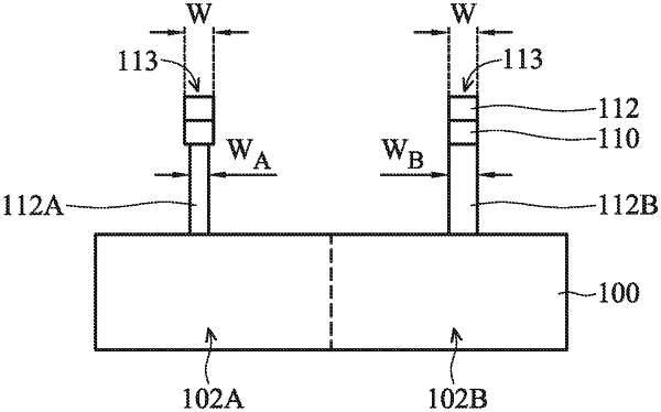
simultaneously etching the p-type silicon layer to have a first width and the n-type silicon germanium layer to have a second width that is less than the first width, wherein the etched p-type silicon layer having the first width is a p-type silicon fin and the etched n-type silicon germanium layer having the second width is an n-type silicon germanium fin, wherein:
an n-type single-fin transistor of the CMOS transistor includes the p-type silicon fin and a p-type single-fin transistor of the CMOS transistor includes the n-type silicon germanium fin, and
the p-type silicon layer and the n-type silicon germanium layer are simultaneously etched to have an etched width difference between the first width and the second width that is 0.5 nm to 3 nm and an etched width ratio of the first width to the second width that is 1.1 to 1.3;
forming a gate that wraps a channel portion of the p-type silicon fin and a channel portion of the n-type silicon germanium fin, wherein the gate is shared by the n-type single-fin transistor and the p-type single-fin transistor;
recessing source/drain portions of the p-type silicon fin and recessing source/drain portions of the n-type silicon germanium fin; and
forming n-type epitaxial source/drain structures on the recessed source/drain portions of the p-type silicon fin and p-type epitaxial source/drain structures on the recessed source/drain portions of the n-type silicon germanium fin, wherein the n-type single-fin transistor includes the n-type epitaxial source/drain structures and the p-type single-fin transistor includes the p-type epitaxial source/drain structures.
|